Superconducting contacts to WTe2 via Pd diffusion
13.09.2022A Swiss-US-Japan collaboration involving the nanoelectronic group and the SNI NanoImaging lab at the University of Basel, the Swiss Federal Laboratories for Material Science and Technology (EMPA), the Department of Materials Science and Engineering and the Department of Physics at the University of Tennessee, the Material Science and Technology Division of the Oak Ridge Laboratories, USA, and the National Institute for Materials Science at Tsukuba, Japan, have found an elegant way to realize highly transmissive superconducting contacts to WTe2: read further the article .This is achieved via Pd contacts which are themselves not sperconductors. However, in contact with WTe2, Pd starts to interdiffuse with W leading to a new crystalline compound that is a superconductor.
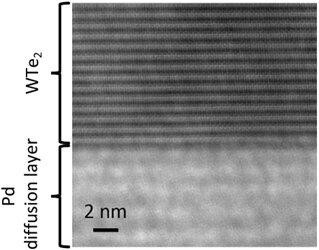
Amazing is the sharp interfacebetween this alloyed superconductor and the remaining WTe2 crystal (see image at the right — actually one of the first images taking with the new JEOL STEM at the SNI NI-lab). This clean interface gives hope to soon confirm that WTe2 is a higher-order topological insulator, predicated by theory. The next step will be to use these contacts to study high quality Josephson junctions (weak links) realized in WTe2 and to search for the fractional Josephson effect and the related 4pi perdiodicity in the current-phase relation.
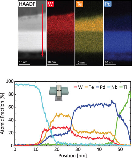
In honour to our SNI NI-team, who made the new JEOL STEM quickly accessible, we post here at the bottom also a STEM cut with EDX material analysis. Note, that the bottom diffusion layer covers more than half of the original WTe2 crystal thickness. It is clear from the EDX signal that the amount of W has been reduced and that there is now a large concentration of Pd found in that region forming the superconducting contact.